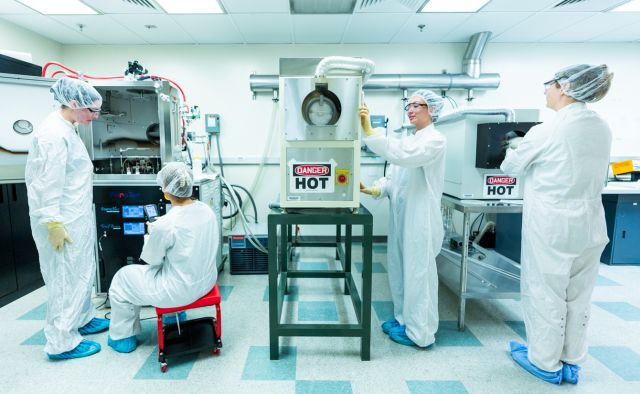
ECE Teaching Cleanroom
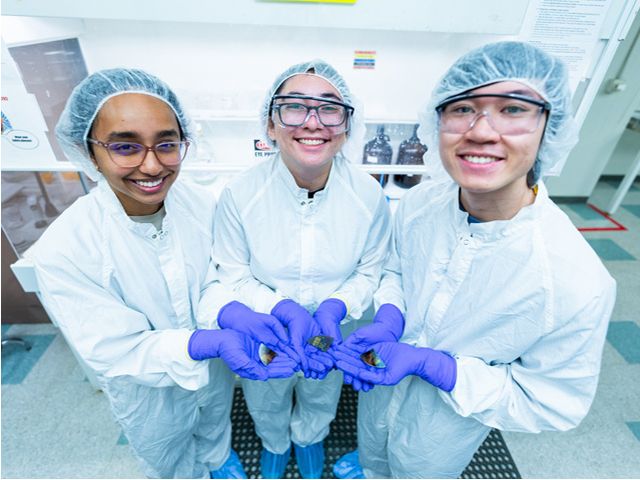
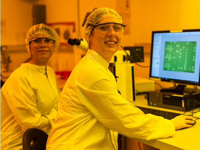
At the UCSB Teaching Cleanroom, students transform classroom concepts into real semiconductor devices. Graduate researchers, future engineers, and trainee technicians gain hands-on experience fabricating and characterizing technologies ranging from MOS capacitors and MOSFETs to HEMTs, MEMS microfluidic structures, and GaN LEDs. This environment prepares students for advanced careers in micro- and nano-fabrication, while giving visitors and parents a clear view of how foundational coursework translates directly into innovation.
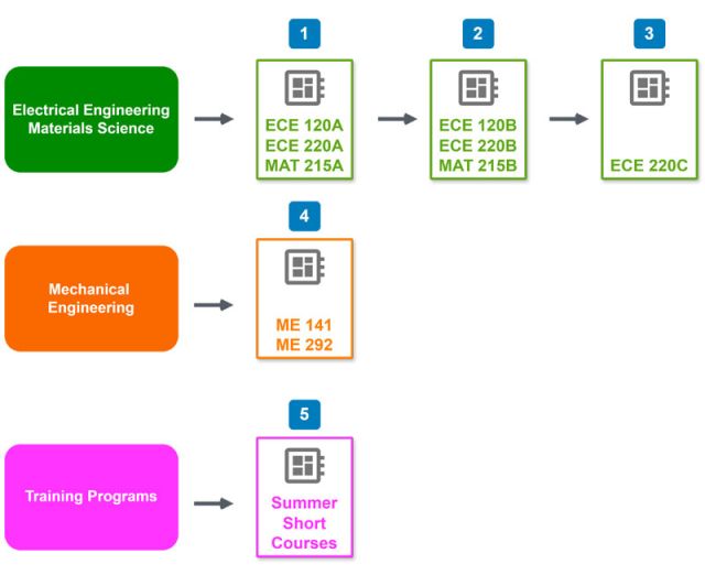
The facility supports a range of microfabrication courses, including ECE 120A, ECE 220A / MAT 215A, ECE 220B / MAT 215B, and ME 141. Academic users intending to work in the Nanofab are strongly encouraged to complete at least one introductory course (ECE 120A or ECE 220A).
Facility Info
Hours: Open Mon – Fri from 9:00 am to 6:00 pm
Location: Engineering II, Bldg 503, Rm 1141
Phone: (805) 893-4142
Access: Keycard only. Prior authorization and training is required.
Important
The TCR is for teaching and training-related activities only. Please contact the UCSB Nanofab for research activities.
Summer Programs
We offer summer courses in advanced manufacturing geared towards technicians. Please enroll with PaCE.
- Microchip Fabrication - I: An intense short-course in nMOS device fabrication and testing for technicians.
- Equipment Maintenance Technician Training: A program focused on maintaining and servicing cleanroom tools.
Contacts
Prashant Srinivasan, Cleanroom Manager – prashant@ucsb.edu
Christopher Wimmel, Building Manager – christopherwimmel@ucsb.edu
Student Interns
We are always seeking skilled student interns with backgrounds in CAD, electronics, and hands-on fabrication. Join us to support real semiconductor device builds and gain industry-relevant cleanroom experience.
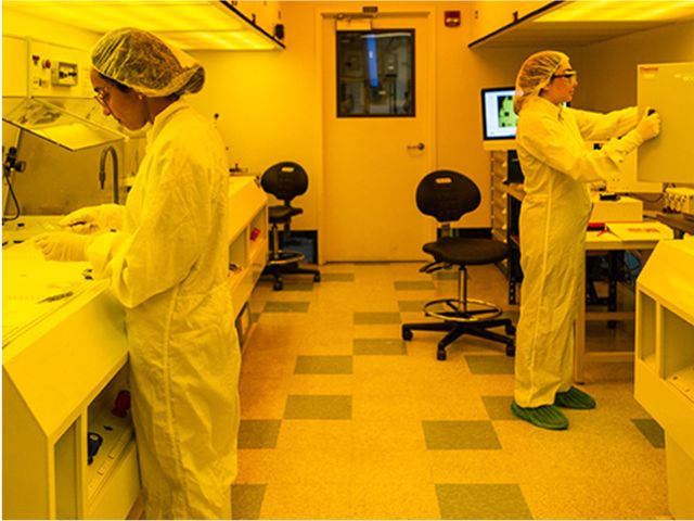
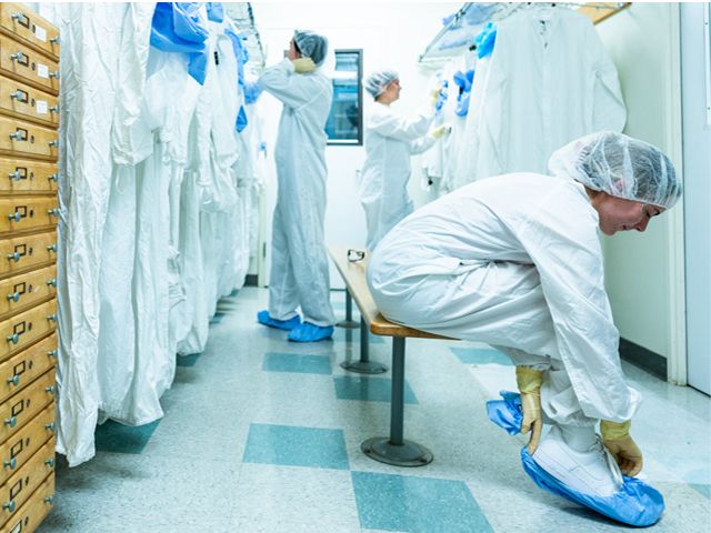
Tools and Instrumentation
- Wet benches – 4
- Spin coaters (Laurell WS-650) – 4
- Ovens (Thermofisher PR305) – 2
- Acid benches – 2 (RCA, HF)
- Oxide growth furnace (MRL 906HT) – 1
- Diffusion furnace (Thermofisher Lindberg BlueM) – 1
- Electron beam deposition (Temescal TLab) – 1
- Plasma Asher (Glow, MRC) – 2
- Annealing station – 1
- MRC-51 Dry Etch (CHF3, CF4, O2, Ar, SF6) - 1
- Electrical characterization stations (Signatone, Alessi) – 4
- Semiconductor Test Equipment (HP4145,4280, 4262) – 4
- Source Measure Units (Keithly 2400, 2440, 2601) – 5
- Contact Mask Aligner (Karl Suss MJB3) – 3
- Profilometers (KLA Alphastep D300) – 2
- Thin Film analyzer (Filmetrics F20) –1
- Ellipsometers (Rudolph AutoEL, J.A. Wollam) – 2
- Microscopes (Zeiss Axioscope) – 4
- Atomic Force Microscope (Nanosurf Easyscan 2) – 1
- Plasma Etcher with SF6,CHF3,CF4,Ar, O2 ( MRC RIE 55) - 1
- Four Point Probe setups - 4
- Optical Spectrum Analyzer (Agilent 86142B) - 1
Courses Offered
Instructional Microfabrication Laboratory
Electronics, Optoelectronics, Microfluids, Microelectromechanical Systems (MEMS)
We prepare students for a foray into the world of microchip fabrication and beyond, with comprehensive hands-on training in an advanced semiconductor cleanroom dedicated for instructional use only.
All our students are trained in industry standard practices such as maintaining detailed process travelers, design for manufacturing, fabrication tolerance, tool calibration and passdown protocols.
- Electrical Engineering | Material Science (# 1, 2, 3)
-
Electrical Engineering | Material Science
- Electronic device fabrication: The 1xx series are undergraduate and 2xx are graduate level classes. Students first learn how to safely work in a cleanroom environment, then advance to fabricating metal-oxide semiconductor (MOS) devices with contact Photolithography. Mask plates (device imprints) are provided to the students. This adventure culminates with electrical testing and characterization.
- Advanced fabrication: Builds on the 1xx/2xx series of classes.
120B - Lab to Fab: Hands on application of VLSI design principles. Based on the experience from the previous class, students first propose a device (ex: Half-Adder, N-bit counter, Transistor demodulator), simulate it in SPICE, then layout lithography masks in LEdit/KLayout, send the masks out for fabrication, make their microchip device in the cleanroom, fully characterize it and report their findings. This is a cool class!
220B/215B - Beyond Silicon: High Electron Mobility device fabrication. Students move beyond Silicon and fabricate and characterize multi-stack GaAs devices.
- Optoelectronic device fabrication: Builds on the 1xx/2xx series of classes.
220C: Students enter the exciting world of fabricating light emitting devices based on GaN substrates.
- Electronic device fabrication: The 1xx series are undergraduate and 2xx are graduate level classes. Students first learn how to safely work in a cleanroom environment, then advance to fabricating metal-oxide semiconductor (MOS) devices with contact Photolithography. Mask plates (device imprints) are provided to the students. This adventure culminates with electrical testing and characterization.
- Mechanical Engineering (# 4)
-
Mechanical Engineering
4. Microfluidics/MEMS fabrication: The 1xx series are undergraduate and 2xx are graduate level classes. Students first learn how to safely work in a cleanroom environment, then advance to fabricating micromechanical devices such as microfluidic pumps and sensors with contact Photolithography and finally characterize their devices by optical and electrical techniques.
- Training Programs (# 5)
-
Training Programs
5. Accelerated Training Programs: Typically 8 week long summer programs ranging from bootcamps for new entrants to semiconductor fabrication and advanced training for working professionals. New courses are continuously being developed. Tracks include the technician training program, upskilling for engineers and students/researcher bootcamps for internal users.You do not have to be a UCSB student to enroll in these programs. Offered in partnership with PaCE, UCSB Nanofab and the CNSI. Please contact us directly for your needs. Current offerings include Microchip Fabrication - I and Equipment Maintenance Technician Training. Register at PaCE.
Safety
- The ECE Electronics Shop maintains safety training records. Safety training is required for lab access.
- Environmental health and safety offers safety training classes at their facility that occur every quarter, however due to COVID-19 live classes are currently not available. Please visit the UC Learning Center to sign up for the online Safety Training courses.
Learn more about Required Safety Training and Reporting Lab Safety Issues on the ECE Electronics Shop webpage